Samsung Invests $280 Million in Japan: Building a Chip Packaging Powerhouse
News Synopsis
Samsung Electronics is poised to establish a groundbreaking chip packaging research unit in Japan, marking a significant investment of approximately 40 billion yen ($280 million) over the forthcoming five years. This strategic move, announced by the city of Yokohama, underscores Samsung's ambitious plans to advance chip packaging technology.
Samsung's Investment in Yokohama
Samsung's decision to set up this research facility aligns with its intention to dive into progressive chip packaging research. Reports earlier in March hinted at Samsung's interest in establishing a packaging center in Kanagawa prefecture, leveraging strong associations with Japanese chip manufacturing equipment and materials suppliers.
Global Collaboration and Technological Competition
This initiative echoes the broader global trend where corporations are joining forces to counterbalance China's burgeoning technological dominance. Amidst improving relations between South Korea and Japan, Samsung's strategic investment in Japan signifies a shift towards reinforcing technological prowess and fostering innovation.
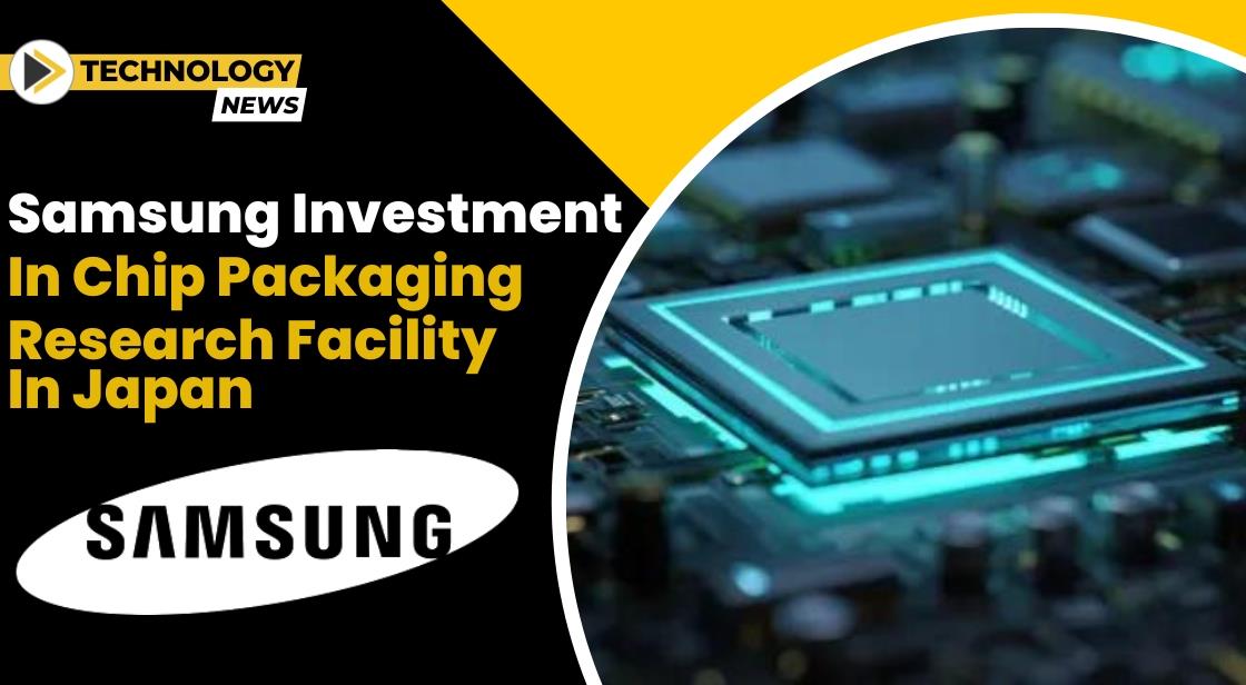
Focus on Semiconductor Advancements
Within the competitive semiconductor landscape, companies are relentlessly pursuing advancements in cutting-edge packaging techniques. These techniques involve amalgamating diverse components into a single package, promising amplified chip performance and efficiency.
Samsung's Commitment to Technological Leadership
The substantial investment in the Japanese research facility not only underscores Samsung's dedication to technological progress but also emphasizes its quest for leadership in the chip industry. By collaborating with Yokohama-based firms specializing in packaging technologies, Samsung aims to fuel innovation and maintain its competitive edge in the dynamic semiconductor market.
Leadership Vision in Chip Development
Kyung Kye-hyun, the head of Samsung's chip business, highlighted the critical role of this facility in fostering collaboration and spearheading advancements in the ever-evolving domain of chip development.
Packing a Punch in Chip Performance:
In the ever-evolving world of semiconductors, advanced packaging techniques are emerging as game-changers. These intricate processes involve miniaturized stacking and integration of various components onto a single chip, boosting overall performance and efficiency. Samsung's investment in Japan underscores its dedication to staying ahead of the curve in this critical area.
Leadership Through Synergy:
Beyond technological advancement, Samsung's Japanese foray aims to solidify its leadership position in the global chip market. By partnering with Yokohama-based companies specializing in packaging technologies, Samsung hopes to leverage their expertise and create a synergistic ecosystem of innovation, keeping them ahead of the pack in the dynamic semiconductor race.
Collaboration is Key:
Kyung Kye-hyun, head of Samsung's chip business, emphasized the facility's role in strengthening collaboration and solidifying leadership in the fast-paced field of chip development. This commitment to partnerships could pave the way for a new era of collaborative innovation in the global semiconductor landscape.
You May Like